
Whenever a reduced process is available to chip designers, there are several different levers they can use to create a more powerful compute engine. With NEC’s latest “Aurora” vector engine accelerators, longtime supercomputer maker NEC is pulling a bunch of levers all at once – and apparently to varying degrees to keep the chips from getting too hot.
We say apparently there because NEC’s announcement was pretty thin on the details. We asked specific questions about the new VE30, the third generation of Vector Engine accelerators to come out of NEC in the last five years and the latest in a long, long line of Vector Engines that goes back as far as you can remember. But so far, NEC has not responded.
In the meantime, as has happened before with Vector Engine announcements, we’ll tell you what we know and infer a bit to try to fill in some of the gaps.
Let’s first look at the NEC Aurora Accelerator roadmap:
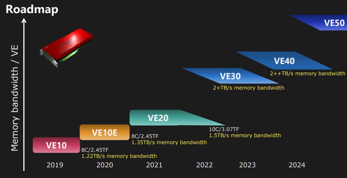
There are actually several iterations in each VE family, and all of them are based on HBM2 memory so far. Generally speaking, NEC has focused on increasing memory bandwidth with each generation and increasing computing capacity wherever possible. With the VE30 generation, expected around 2022, the roadmap promised to deliver over 2TB/sec of memory bandwidth on every device, which is there with the latest GPU accelerators on the market used for HPC and AI workloads . To be precise, the NEC roadmap called for the VE30 to have a “new architecture, larger memory bandwidth, higher core count, higher frequency, and new functions”.
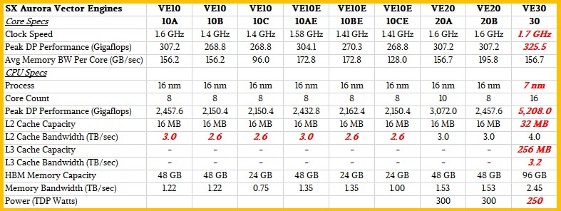
Here’s what we know. The number of cores in the VE30 is 16, compared to the 10 cores of the VE20, and the memory bandwidth has increased by 1.6 times and the memory capacity has increased by 2 times. If you do the math on all that, then the 16-core VE30 vector math accelerator has 96GB of HBM2e memory (we’re assuming NEC hasn’t made an aggressive transition to HBM3 like Nvidia is saving it for upgrade upgraded to VE40 coming next year) and boasts 2.45 GB/s of aggregate bandwidth from that HBM2e memory.
Although NEC hasn’t specified any of this, we believe it has gone from a 16 nanometer process from Taiwan Semiconductor Manufacturing Co used with the Aurora family VE10 and VE20 accelerators to a reasonably mature 7 nanometer process. from TSMC. There’s no way NEC went for TSMC’s 10 nanometer shrinkage – that node wasn’t really used in high-performance devices and was tough as it has been for Intel and GlobalFoundries. And we don’t think NEC would move to a 5 nanometer process and there’s no way they would be first in line with a 3 nanometer process. These processes are too expensive to use for relatively low volume products in a very limited market size. (Nvidia can push the envelope as thousands of HPC and AI customers use its data center GPU compute engines.)
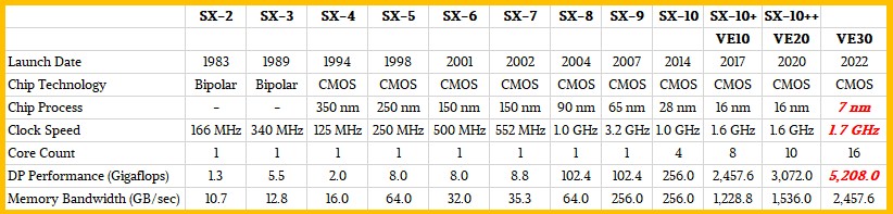
The other data we know is that Tohoku University in Japan, which has been using NEC SX series vector supercomputers since the announcement of the SX-1 and SX-2 in 1983, is going to take delivery of a stuffed supercomputer of 4,032 of these VE30 engines which should be rated at around 21 petaflops of maximum aggregate floating point computation with 64-bit precision. This will make Tohoku University’s machine the most powerful vector supercomputer in the world, and in all of computing history, and it will be 586 times more powerful than the 35.86 teraflop Earth Simulator that NEC has built for the JAMSTEC laboratory in Japan in 2001.
If you do the math backwards, a 16-core VE30 vector accelerator is rated at 5,208 gigaflops, which means that the maximum FP64 performance per core on the VE30 is 325.5 gigaflops. That’s just under a 6% performance increase per core over a VE20 vector accelerator core. Which means that the clock speed of the VE30 is only 6% faster than the 1.6 GHz of the VE20.
This relatively low clock speed, if we’ve deduced it, is a little surprising at first, but not considering that most HPC centers are as concerned about performance per watt as they are about performance as electricity is not cheap.
Moving from TSMC’s 16 nanometer process to its 7 nanometer process – what it calls a full node hop – provided clock speeds between 35-40% faster on transistors in the same power envelope or 65% lower power consumption at the same clock speed and 3.3 times higher transistor density factor. Rather than crank the clocks all the way up and create a huge 16-core package that runs at 600 watts or even 700 watts, NEC seems to have increased the clock speed slightly with the VE30, doubled the cores (possibly with a multi- chip module approach that would be a simpler design and would allow memory capacity to be doubled while increasing memory bandwidth by 1.6X – and would in fact reduce overall power consumption.
Here is our best guess on how the VE30 vector accelerator compares to its predecessors in the Aurora line:
And here’s how this generation VE30 compares to the SX-2 engines made by NEC:
NEC said it added L3 cache to the VE30 architecture, which we assume is a shared cache for all cores, as is the case with CPUs and GPUs these days. No details were given on this L3 cache, but if the cache resembles that of modern CPUs and GPUs, it should be a factor of 4X to 8X larger than L2 cache and it should have less aggregate bandwidth than L2 cache but more aggregated bandwidth than HBM2e memory. We’ve tried it and think the L3 has 256MB of capacity and 3.2TB/sec of aggregate bandwidth. (We admit that’s a wild guess.) The important thing is that the accelerator has 2.45 GB/sec of HBM2e bandwidth that can pump data like crazy into that L3 cache, allowing for better balance data moving in the L2 cache. (We suppose.)
Frankly, we are surprised that there is an L3 cache and NEC specifies that this is the first time in its vector architecture that it uses an L3 cache. Processors have a large L3 cache because DDR DRAM is too slow compared to L2 cache. But that’s not the case with L2 cache versus HBM2 and HBM2e memory, so it’s a confusing choice.
We don’t have many processors with HBM, HBM2 and HBM2e memory to take as examples. Fujitsu’s Sparc64-XIfx processor used in its supercomputers several years after the launch of the “K” supercomputer had eight HBM blocks with 2.2 TB/sec of L2 cache bandwidth directly linked to eight HBM1 banks with 480 GB/sec of bandwidth. Fujitsu’s A64FX processor used in the “Fugaku” supercomputer had 3.6 TB/sec of L2 cache bandwidth powered by 1 TB/sec of HBM2 memory consisting of four blocks running at 256 GB/sec.
Nvidia, AMD, and Intel discrete GPUs have L2 cache memory and various HBM memories, but no L3 cache memory.
Presumably, Intel will ship L3 cache on the HBM version of its “Sapphire Rapids” Xeon SP processor, now expected early next year if the rumors are correct. But as far as we know, L3 cache will be disabled and L2 will be tied directly to HBM memory somehow.
As we said, it’s an odd choice to add L3 cache to the VE30 compute engine, and we can’t wait to hear more.
A few other things. It was rumored last year that the VE30 motors would not only support FP64 double-precision and FP32 single-precision calculations, but also FP16 half-precision calculations. The latter would make Aurora engines suitable for running machine learning training workloads, which could be useful in developing the market for these chips. Also, we assume that the VE30 acceleration engine comes with a PCI-Express 4.0 x16 slot, not the PCI-Express 3.0 x16 slot used by previous generations. And next year, the VE40 should probably have a PCI-Express 5.0 slot and also support the CXL 2.0 protocol. Why not?
#Cores #clocks #caches #launched #latest #NEC #vector #engines